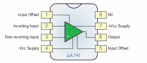
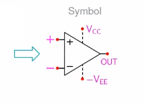
Operational amplifier has two inputs, Inverting (-ve) and non inverting (+ve) inputs and one output. 741 is one of the traditional op-amp, which have 8 pins. two pins are inputs, one pin is output and a Vcc (+ve) and Vee (-ve), which are supply voltages (range 5 to 15 V). It also have two offset pins which is used for op-amp adjustments. remaining one pin in 741 is not connected.
Contents
Ideal and Practical Opamp
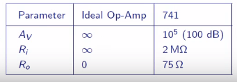
Ri = input resistance
Ro = Output resistance
Also the voltage gain and bandwidth of an ideal amplifier is infinite. But for practical amplifier voltage gain and bandwidth are very high values (not infinity).
Output voltage of an Op-amp is in between +Vsat and -Vsat. Where Vsat or saturation voltage is 1.5 V less than supply voltage. Input voltage of an op-amp is very small (milli volt range) because this pins are connected to base of two transistors (from internal diagram of Op-amp).
Op-amp have two regions namely linear and saturation region. Thus Op-amp operation can be classified into two
- Op-amp operating in linear region
- Op-amp operating in saturation region
An op-amp in a circuit is operating in linear region or saturation region. Which depends upon magnitude of input voltage and feed back of Op-amp (negative or positive feedback).
\(V_o = A_v (V_+ – V_-)\)
\(A_v\) is the voltage gain which can also be represented as \(A_d\) or differential gain because it is multiplying with difference of inputs. Since input resistance of op-amp is infinity so input current will be zero. Also input voltages \(V_+\) and \(V_-\) are almost similar.
Common mode and Differential mode
In common mode, input signals applied to both inverting and non inverting terminals are identical. That is it have same amplitude, frequency and phase difference. The resultant output is zero, Because it cancels each other. This property is called common mode rejection.
Differential mode is of two types. single ended differential mode and double ended differential mode. In single ended differential mode, one input is grounded and other is feed with a signal. If signal is connected to inverting terminal, we get an inverted signal at output. similarly if connected signal to non inverting terminal, a non inverted signal is obtained at output. In case of double ended differential mode, both inputs are feed with opposite polarity signals and output will be the difference between this two signals.
common mode voltage \(V_c = \frac{1}{2}(V_1 + V_2)\)
differential voltage \(V_d = (V_1 -V_2)\)
From the above two equations we can say that common mode voltage is higher than differential voltage.
In practice output voltage also have a common mode factor.
\(V_o = A_d V_d + A_c V_c\)
\(A_c\) is common mode gain, which we make very low because ideally we don’t need this common mode factor.
The ability of an amplifier to reject common mode signal is called Common Mode Rejection Ratio or CMRR
CMRR = \(\frac{A_d}{A_c}\)
CMRR in db = 20 \(log( \frac{A_d}{A_c})\)
Ideal value of CMRR is infinity and practically very large. It should be very large to avoid unwanted common mode signal from the output. practical value of CMRR IS ABOUT 30,000 or 90 db.
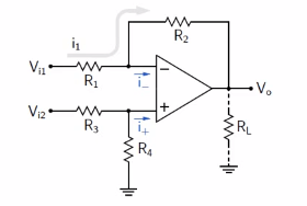
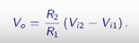
Difference Amplifier
Can above described OP-amp be used itself as a difference amplifier ? No is the answer, because of two reasons
- First reason : gain of op-amp is very high, so differential inputs of an op-amp should be small, otherwise positive or negative saturation occurs.
- Second reason : Is due to offset voltage of op-amp.
Thus we make a circuit with op-amp to form difference amplifier.
Parameters of Opamp
Open loop voltage gain
It is ratio of output voltage of op-amp to input signal, in which no external components are connected. Some times it is also called large signal voltage gain. Its typical value is around 2,00,000
Maximum output voltage swing
When no inputs are connected to both the input terminals then the output of the op-amp will be ideally zero and this is called quiescent output voltage. If we connect input signals then peak to peak output of the op-amp should be ideally \(\pm V_{cc}\). but practically this voltage swing is not correct because of the load resistance. This voltage swing is directly proportional load resistance.
Input offset voltage
When we applied zero input signals, ideal output is zero. But practically we will get a small error voltage and it is called input offset voltage. typical value is 2 mV or less. This is due to the mismatch in the input terminals which are actually two bases of a differential amplifier (internal structure of op-amp). There is an another term called Input offset voltage drift, It is the rate of change of offset voltage with temperature.
Input bias current
We already discussed that input of op-amp is input to base of differential amplifier. input bias current is the current supplied to this two base for proper biasing of transistors in differential amplifier. This is equal to average value of the the two input currents.
Input Offset current
Ideally two input currents are same. thus its difference is zero. But in practical their is slight difference between them. this difference is called input offset current.
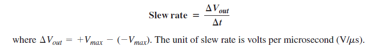
Slew Rate
It is the maximum rate of change of output signal with respect to change in input signal. In other words, It is the change in output voltage in certain interval of time.
Why we use negative feedback in op-amp circuit
Negative feedback is a process of feeding a portion of output to the input in opposing phase angle with input signal. That is there should be a phase difference of 180 degree between the feedback and input signal.
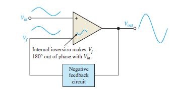
Op-amp circuit with feedback is called closed circuit and op-amp without feedback is called open circuit op-amp. In case of open-circuit, even a small noise generate large output (saturation) because of the high voltage gain of op-amp (more than 1,00,000). So open loop op-amp circuit is only used in op-amp comparator circuits. In closed loop op-amp circuit with negative feedback, we can avoid an op-amp which became saturation state even with small signals. Thus with negative feedback we can control op-amp voltage gain. Negative feedback also provides control of the input and output impedances, amplifier bandwidth and frequency response.
Non-Inverting amplifier circuit of opamp
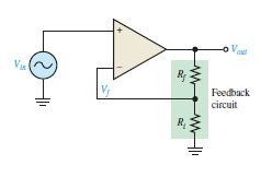
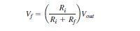
In non-inverting amplifier, input signal is feed directly to non inverting terminal of opamp and feed back is feed into inverting terminal as shown in the figure. This feed back signal \(V_f\) is
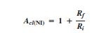
closed loop gain is independent of open loop gain and it can represented by an equation,
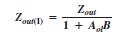
Input impedance and out put impedance of non inverting amplifier is,
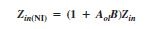
Input impedance of the non inverting amplifier circuit with negative feedback is much greater than the internal input impedance of the op-amp
itself (without feedback).
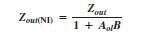
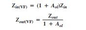
Voltage-Follower in opamp
Voltage-Follower is a special case non inverting amplifier. Here all the output voltage is feed in to input section. So closed loop gain is unity , input impedance is very high and output impedance is very low. These features make it an ideal buffer amplifier for interfacing high-impedance sources and low-impedance loads.
Inverting Amplifier in opamp
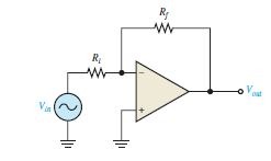
It has a Negative feedback with an input signal connected to inverting terminal and non inverting terminal is grounded. Input impedance of an ideal op-amp is infinity so input current is zero. if input current is zero, then potential difference between inverting and non inverting terminal is zero. Since non inverting terminal is grounded. so voltage at inverting terminal is also zero. this zero potential is called virtual ground.
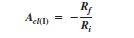
the closed-loop voltage gain of the inverting amplifier is the ratio of the feedback resistance to the input resistance.