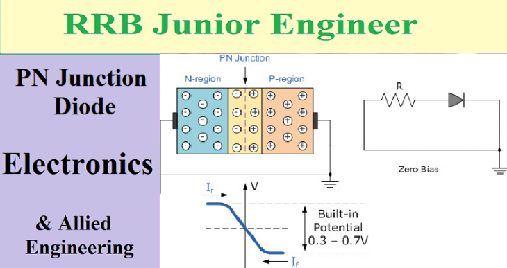
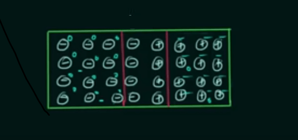
PN junction Diode is formed by joining P type semi conductor and n type semiconductors. Due to diffusion of electrons and holes from P region and N region a depletion layer is formed in between P type and N type semiconductors. This region consist of positive and negative ions. Where positive ions aligned on the N type side and negative ions on the P type. which you can see in the below figure. These ions are immobile and and are covalent bonds. Dimension of depletion region is 0.5 micro meter.
PN Junction Diode possess the properties of a RECTIFIER
Contents
Depletion region in diode
Depletion region restrict the movement of majority carriers across the junction. So holes from P type and electrons in the N type is blocked by depletion region. But it allows the movement of minority charge carriers. That is it allow electrons in P type and holes in N type to pass across the depletion region. Other names of depletion layer are Space charge width and Transition layer. We cannot measure depletion voltage using a voltmeter because, voltmeter have a high resistance in series.
Depletion width \(\alpha\) \(\frac{1}{\sqrt[]{Doping}}\)
From above equation we have the relation between depletion width and doping . When doping increases width of depletion layer decreases. Minority carrier flow through depletion region results in a current called leakage current or Drift current. This leakage current is negligibly low. Diffusion current is current due to majority charge carriers. This diffusion current and drift current will become equal at steady state condition.
Electric field is maximum in the mid portion of the depletion region. That’s why depletion layer decreases while doping increases
Barrier Potential
When we connect a cell across a PN Junction Diode (in reverse or forward direction) depletion layer becomes potential barrier. Potential barrier can be represented by some other terms like Built-in potential, Built-in voltage, potential hill, contact potential, Diffusion voltage.
Barrier Potential formula is,
\(V_o\) = \(V_t \log_e{\frac{N_a N_b}{n_i^2}}\)
\(V_o\) = Barrier potential
\(V_t\) = Thermal voltage
\(N_a\) = Acceptor concentration
\(N_d\) = Donor concentration
\(n_i\) = Intrinsic concentration
Potential barrier of holes increases from depletion region at the p type to N type. similarly potential barrier of electrons increase from depletion region at the n type to p type.
At room temperature Thermal voltage of silicon diode is 0.7 V and for germanium is 0.35 V. This potential exist even if the diode is not connected to any supply.
We can calculate width of depletion region using Barrier potential. It is represented in meter. Equation for Depletion with is
W = \(\sqrt{\frac{2 \epsilon}{q}[\frac{1}{N_a}+\frac{1}{N_d}]V_o}\)
\(\epsilon\) = Permitivity
\(N_a\) = Acceptor concentration
\(N_d\) = Donor concentration
\(V_o\) = Barrier potential
q = charge of carrier
Forward Biased Diode
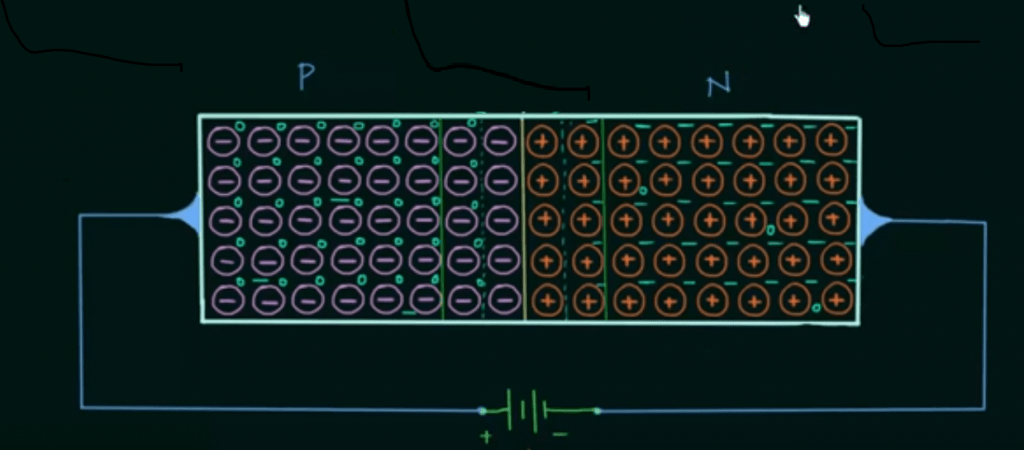
In forward biased condition a DC supply is provided across PN junction diode. Where positive terminal of the supply is connected to P type semiconductor and negative terminal to N type semiconductor. Holes (majority) in the P type repelled to depletion layer by the positive terminal (like charge repels) of the cell. It is combined with the immobile negative ions .
Similarly, electrons (majority) in the N type semiconductor repelled towards depletion layer by the negative terminal of the cell. In the depletion region it is combined with the immobile positive ions . Thus width of the depletion region decreases. More importantly diode current will start to conduct in forward bias from P to N.
Diode current is the difference between current due to majority charge carrier and minority charge carrier. This minority charge carrier current is called reverse saturation current. Reverse saturation current is very low and completely depends on temperature. As temperature increase reverse saturation current also increases.
When forward bias is applied across a PN Junction diode, its Depletion region decreases
After forward biasing barrier potential of the diode changes.
Barrier potential ( forward bias ) = \(V_b – V_s\)
\(V_b\) = barrier potential at non biased condition
\(V_s\) = supply voltage
when \(V_b\) = \(V_s\) , diode current start flowing. \(V_b\) of silicon is 0.7 V, if supply voltage is 0.7, current starts flowing.
Reverse Biased Diode
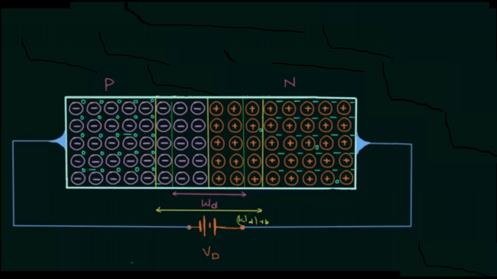
In reverse biased condition a DC supply is provided across PN junction diode. Holes (majority) in the P type is attracted from depletion layer to the negative terminal (unlike charge attracts) of the cell.
Similarly electrons (majority) in the N type will be attracted towards negative terminal of the cell from depletion layer. Thus width of the depletion region increases. Width of depletion layer is maximum in reverse biased condition and minimum in forward biased condition. Diode current current due to majority carrier become zero, because of the increased depletion layer width. But the flow of minority charge carriers does not change so their will be an extremely low reverse saturation current in the order of micro ampere.
Barrier potential ( reverse bias ) = \(V_b + V_s\)
\(V_b\) = barrier potential at non biased condition
\(V_s\) = supply voltage
VI Characteristics of PN Junction Diode
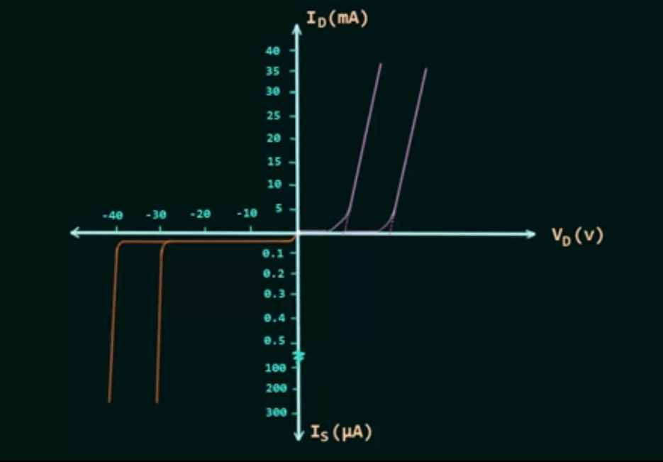
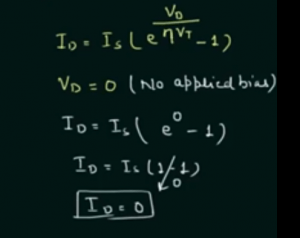
\(V_D\) in the diagram is the supply voltage. when \(V_D\) is zero, diode current also become zero.
When we increase supply voltage from zero, diode current increases exponentially after reaching the barrier potential (Ge = 0.3 V & Si = 0.7 V). During negative bias condition majority current become zero and saturation current remains unchanged (negligible saturation current is always present in all condition). when we increase the negative potential of the supply to a particular value called Break down voltage or zenor voltage, break down of diode take place. During break down some electrons breaks its covalent bond and become free, these free electron hit other atom’s electron. This chain process continue and as a result reverse saturation current increases exponentially.
Peak Inverse Voltage – It is the maximum reverse voltage that we can apply across a diode, before it enters break down or Zenor region.
Effect of Temperature on V-I characteristics
According to temperature V-I characteristics of diode changes. In case of forward biased region, characteristics of Silicon diode shifts to the left at a rate of 2.5 mV per degree Celsius rise in temperature. similarly It shift to the right in same rate when temperature decreases.
For reverse biased condition, reverse saturation current doubles for every 10 degree temperature rise. It is dangerous, it may fail the diode. To avoid this we use diodes with 10 pico ampere saturation in high temperature application. As temperature increases Break down voltage increase or decrease according to Zenor value.
Germanium diode is not used in high temperature conditions. Because of its increased reverse saturation current. GaAs and Si have love reverse saturation current
Thanks on your marvelous posting! I seriously enjoyed reading it, you’re a great author.I will ensure that I bookmark your blog and may come back later on.
I want to encourage you continue your great posts, have a nice afternoon!
Here is my web page: Ozempic