
This post contains all the theoretical explanations of conductor, semiconductor and insulator, followed by a Mock Test with Multiple Choice Questions .
Contents
Difference between Conductor, Semiconductor and insulator
| parameter | Conductor | Semiconductor | Insulator |
| Resistance | Low | medium | High |
| Conductance | High | medium | Low |
| Temperature | +ve temp coeff. | -ve temp coeff. | -ve temp coeff. |
| Current | High | medium | Low |
| Free electrons | Very High | medium | Low |
| Bond | metalic bond | Covalent bond | Ionic bond |
| Band gap | Zero | Si = 1.14, Ge =0.67 (less than 2 ev) | greater than 6 eV |
Materials are classified into conductors, insulators and semiconductors. This classification is based on the conductivity of material. Conductors have high conductance (Iron, Copper, Silver etc.,) hence it got that name. insulators have poor conductance (Wood, paper etc..). Conductance of semiconductor is in between conductor & insulator and it is used in manufacturing of electronic components (silicon, germanium). Conductance is denoted by G.
In terms of Resistance, which is opposite of conductance. in other words resistance is inversely proportional to conductance. That is
Resistance \(\alpha \) \(\frac{1}{conductance}\) .
So Resistance is high in insulator, low in conductor and medium in semiconductor. Resistance is denoted by R.
As Temperature of a Conductor increases its resistance also increases. thus we can say Conductors have positive temperature coefficient. Insulator and Semiconductor have negative temperature coefficient, because here temperature and resistance are inversely proportional. That is when temperature increases resistance decreases.
Conduction Band and Valance Band
There are two bands in materials. which are conduction and valance band. conductivity depends on number of electrons present in conduction band. these electrons are called free electrons. Electron in the valance band jumps to conduction band, then conduction take place.
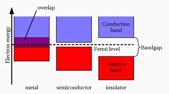
Gap between conduction and valance band is called Forbidden gap. imaginary line drawn between these bands are called Fermi level. In metal or conductor two bands overlap each other. In semi conductor band gap is very small. Large band gap is present in insulators, so it is difficult for an electron to jump from valance band to conduction band.
Semiconductor Classification
Semi conductors are classified in three ways.
- Direct and Indirect Band gap semiconductor
- Elemental and compound semiconductor
- intrinsic and Extrinsic semiconductor
Direct and Indirect band gap semiconductor
electrons in valance band acquire energy and jump to conduction band. This electron will conduct but it is unstable, thus it have a tendency to release energy and returns to valance bond.
If electron falls from conduction band to an intermediate band between conduction and valance band and from their to valance band, then such semiconductors are called Indirect band gap semiconductor. Here heat is emitted during electron movement from conduction to valance band
If electron falls directly from conduction band to valance band, such semiconductors are called direct band gap conductors. Here light is emitted during electron movement from conduction to valance band.
Elemental and compound semiconductor
Semiconductors formed by elements itself is called elemental semiconductor. example : silicon, Germanium. Both the examples are tetravalent elements (elements with four valance electrons).
Semiconductors which are compounds are called compound semiconductor. Here one element of the compound is trivalent element and another one is pentavalent element. Example : Gallium Arsenide, Indium Phosphide etc..
Intrinsic and Extrinsic semiconductor
Intrinsic semiconductor are pure semiconductors. because which does not have impurities. In other words it is not doped with other elements. number of electrons and holes are same. At 0 kelvin it will act as insulator.
Extrinsic semiconductor are impure semiconductors. Because it is doped with an impurity. Here trivalent element or pentavalent element is doped with an intrinsic semiconductor. If trivalent (Boron, Aluminum etc..) is used as impurity then a P type semiconductor will form, which have more number of positive charged holes than negative charged electrons. If pentavalent(phosphorous) is used as impurity then an N type semiconductor will form, which have more number of negative charged electrons than positive charged holes . Pentavalent element donates an electron so it is called donar atom. Trivalent element accepts an electron
In P type semiconductor majority charge carriers are holes and minority charge carriers are electrons. In N type semiconductor majority charge carriers are electrons and minority charge carriers are holes. N type semiconductor is a donor, because it have more number of electrons so it can donate electron. Due to the large number of holes P type semiconductor is an acceptor.
Rank Point
By doping only majority charge carriers will increase. minority charge carriers will be constant
Difference between Silicon and Germanium
| silicon | Germanium (comparatively) |
| leakage current lower | leakage current little higher |
| high power handling | low power handling |
| high temperature handling | low temperature handling |
| Available | less available |
| cheapest | not so cheap |
Multiple Choice Questions
Select your answer and submit to know correct answer and next question. All the questions are previously asked in competitive exams. Answer all the questions to know your final score and verdict