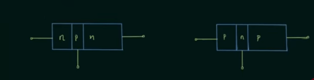
BJT or Bipolar junction transistor consist of three terminals. They are base, emitter and collector. It is used for amplification of weak signals and switching operations. It has two types of physical structures namely PNP and NPN. IN PNP, N type semiconductor is sand-witched between two P type semiconductors. In NPN, P type semiconductor is sand-witched between two P type semiconductors.
NPN transistor is commonly used because mobility of electron is more than mobility of hole
larger region in BJT is Collector region and corresponding terminal is collector terminal. smaller (middle) region is base, Terminal base terminal and medium region is emitter & its terminal is emitter terminal.
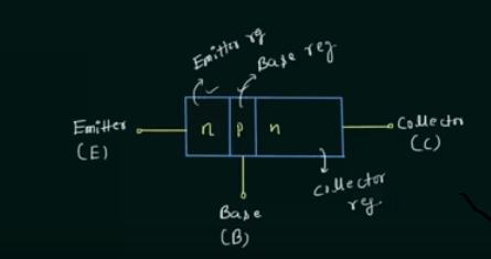
BJT have two junctions, Emitter base junction and collector base junction. Doping in these three regions are different. Emitter is heavily doped, collector is medium doped and base is lightly doped.
Contents
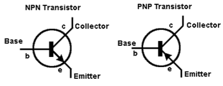
Symbol of bipolar junction transistor
BJT is equivalent to a combination of two diodes connected back to back
Why Bipolar Junction Transistor is called so ?
Bipolar transistor have two types of charge carriers. That is negative electrons and positive holes. hence the name Bipolar. we know that BJT have two junctions hence the name Bipolar junction. Last word transistor is combination of transfer and resistor.
First junction of BJT is forward biased, so low resistance and second junction is reverse biased , so high resistance. Here input signal is feed to low resistance is taken from high resistance region.
Regions of operation of transistor
| Junction 1 | Junction 2 | Region of operation | |
| Forward biased | Reverse biased | Active | Amplification |
| Forward biased | Forward biased | Saturation | ON/closed switch |
| Reverse biased | Forward biased | Inverted | Rarely used |
| Reverse biased | Reverse biased | Cut off | OFF/ Open switch |
Working of a BJT transistor
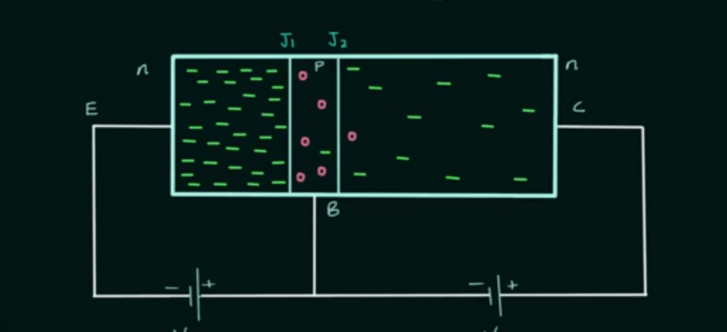
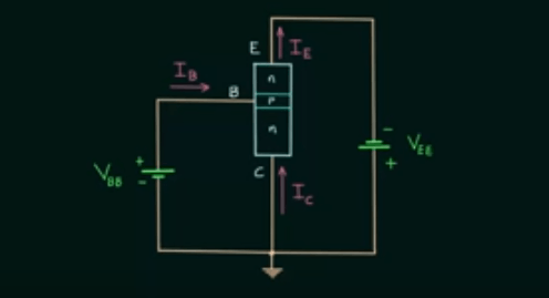
Before biasing two junctions of transistor have same potential which is equal to \(V_b\). When we forward biased the emitter base junction and reverse biased collector base junction as shown in the figure. potential of both the junctions will change. Barrier potential at \(J_1\) = \(V_b\) – \(V_{EB}\) (because in Forward bias barrier potential decrease). Similarly barrier potential at \(J_2\) = \(V_b\) – \(V_{CB}\) (because in reverse bias barrier potential increase).
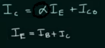
Due to forward biased emitter base, heavily doped electrons move towards base. Base is lightly doped so about 2-5 % electrons combined in base and remaining 95% electrons will be collected in the collector. From these points we will come into the point that current emitter current is 100% , base current 5% of emitter current and collector current is 95% of emitter current.
Junction \(J_2\) is reverse biased so their is reverse saturation current \(I_{CO}\)
Transistor Configurations
There are three types of transistor configurations
- Common Emitter configuration – has both Current and Voltage Gain
- Common Collector configuration – has Current Gain but no Voltage Gain
- Common Base configuration – has Voltage Gain but no Current Gain
Out of this three, Common Emitter is commonly used because of its wide applications. The term common is used to indicate the electrode which is common to input and output.In common emitter, emitter is common to both input and output. because emitter is grounded. Hence these are also known as grounded base, grounded emitter and grounded collector.
| Parameters | common base | common emitter | common collector |
| input resistance (ohm) | 10 | 1 k | 100k |
| Output resistance(ohm) | 100k | 10k | 10 |
| Current gain | \(\alpha\) =0.95 -0.99 | \(\beta \) = 50-500 | \(\gamma \) = 51-501 |
| Voltage gain | very High | medium | 1 |
| Application | RF voltage amplifier | AF voltage amplifier | Buffer impedance matching voltage follower emitter follower |
| Phase change (degree) | 0 | 180 | 0 |
Common Emitter configuration
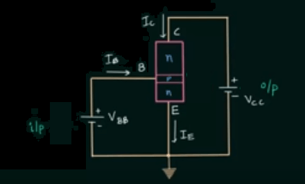
Here input signal is applied at emitter-base side and output taken from emitter-collector. Since CE is used as amplifier so input is made forward biased and out put is reverse biased. common emitter configuration have highest current power gain because of low input resistance high output resistance. \(I_b\) is the input current and \(I_c\) is the output current. Its Current gain is represented by a Greek letter \(\beta \).
\(\beta \) = \(\frac{I_c}{I_b}\).
It is also called common emitter forward transfer ratio. Its value will be in between 50 to 500.
Common Base Configuration
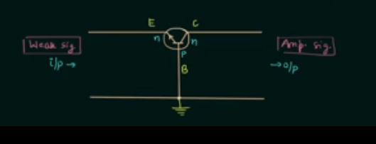
Weak input signal is feed into base emitter side and amplified strong signal is taken from collector base side. So output current is \(I_c\) and input current is \(I_e\). Here current gain is represented by \(\beta\).
\(\beta = \frac{I_c}{I_e}\)
This ratio is also called forward current ratio. Its value is in the range of 0.95 and 0.99. It is widely used as voltage amplifier.
Common Collector Configuration
In this case input signal is applied between base and collector. Output is taken across Emitter and collector.It is also known as emitter follower or collector follower. Here in pot current is \(I_b\) and output current is \(I_e\). current gain is represented by \(\gamma\).
\(\gamma = \frac{I_e}{I_b}\)
Relationship between Alpha, Beta and Gamma
\(\gamma =1+\beta \)
\(\gamma = \frac{\beta}{\alpha} \)
\( \alpha =\frac {\beta }{1+\beta } \)
\( \beta =\frac {\alpha }{1-\alpha } \)
\(I_e : I_b : I_c :: 1 : (1 – \alpha) :\alpha\)
Leakage current in Transistor
In a BJT transistor collector current have two components. One is due to majority charge carriers and another is due to minority charge carriers.
Leakage current is due to the presence of this minority charge carriers.The leakage current is exactly like the reverse saturation current. It is extremely temperature depended. Because it is made of thermally generated minority carriers.